VIA Apollo Pro 266: The P3 gets DDR
by Anand Lal Shimpi on January 18, 2001 2:36 AM EST- Posted in
- CPUs
VIA's Solution: V-Link
Intel identified and addressed this issue back in 1999 with the release of the i810 chipset. The i810 was the first to employ what is now known as the Intel Hub Architecture. To make a long story short, IHA replaces the PCI bus as the connection between the two main parts of the chipset. A bus capable of achieving twice the available bandwidth of the PCI bus replaces it. This bus is an 8-bit wide bus that operates at 133MHz DDR, effectively resulting in 266MB/s of available bandwidth. This interlink bus is present on all 8xx chipsets, including the popular i815.
The "new" way: A dedicated bus connects North &
South Bridges

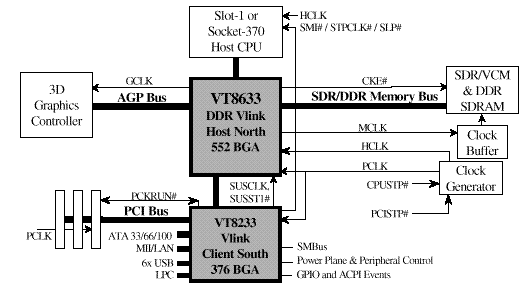
VIA's solution to the problem, albeit a couple of years later than Intel's Hub Architecture, is very similar. Dubbed V-Link, the connection between the North Bridge and the South Bridge is now this interface capable of transfer rates of up to 266MB/s, identical to Intel's interlinks bus.
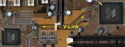
On the Apollo Pro 266 Reference board you can actually see the traces that make up the V-Link bus quite clearly:
Without a need for the PCI bus to connect the two chips it is now moved down to the South Bridge along with the ATA/100, USB and integrated 10/100 Ethernet controllers.
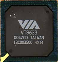
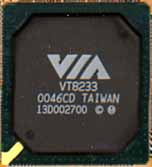
The Apollo Pro 266 in particular is composed of the VT8633 V-Link Host North Bridge and the VT8233 V-Link Client South Bridge. The South Bridge is virtually identical to the 686B from VIA with the exception that it now contains the PCI bus interface, an integrated 10/100 Ethernet controller and supports up to 6 USB ports.
 |
 |


0 Comments
View All Comments